
Program Highlights
Undergraduate Program
Our undergraduate program emphasizes the molecular science aspects of biology and chemistry along with the engineering concepts essential to developing commercial products and processes. Undergraduate Program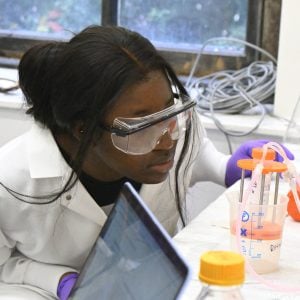
Master’s Program
Deepening knowledge and professional preparation are the focus of our master’s program and students can choose a coursework-only or a research-focused track. Master's Program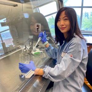
PhD Program
In a research-intensive environment, doctoral candidates are mentored by faculty who are defining their fields and collaborate across university divisions. PhD Program
Concurrent BS/MS program
The concurrent BS/MSE program enables current students to complete both degree is, usually in five years, with a 50% tuition break during their fifth year. Learn moreApply today.
“ChemBE at JHU is tackling our most pressing global challenges in sustainability, climate, and health. Join us in pushing the boundaries of engineering knowledge from the molecular to the systems level. ”
 Jennifer Elisseeff
Professor and interim department head
Jennifer Elisseeff
Professor and interim department head
Vivien Thomas Scholars Initiative
A new doctoral fellowship creating pathways for exceptional students from historically Black colleges and universities and minority-serving institutions to pursue PhDs in STEM fields at Johns Hopkins.
Application deadline: Dec. 1
Learn more about our incredible ChemBE community

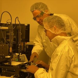
Solving the carbon dioxide problem, one atom at a time - A team led by Chao Wang has developed an innovative way to transform carbon dioxide (CO2) into valuable acetate with remarkable efficiency.

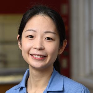
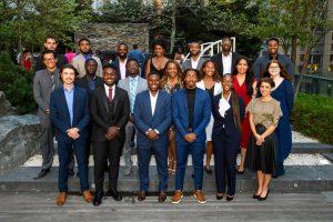
PhD student's team wins top prize in Germany - Doctoral student Anastasia Georgiou and her teammates from all over the world developed a winning concept and business plan at the Merck KGaA Innovation Cup.

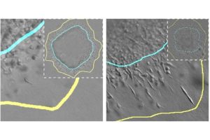
A simple spray could keep COVID-19 away - A team led by Honggang Cui has developed a method to prevent harmful viruses from entering the lungs, blocking them with a nasal spray.
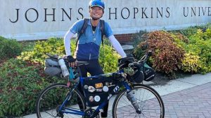
Gearing up for grad school - Doctoral student Chun-Chiao Yang took the long way to his first day of classes, biking over 4,000 miles from San Francisco to Baltimore.
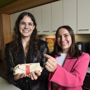
Baltimore is Home - We’re a city rich in history and culture, filled with great restaurants and affordable housing, and because we’re close to so many global companies, career, internship, and research opportunities abound. Baltimore is home.
-

Researchers discover the role of physical forces in the disease’s spread.
-
Chao Wang leads multi-university team under $1M grant from DOE.
-

$625K Department of Energy grant funds system to electrify jets, trains, ships and more.